Zum Inhalt wechseln
SEELANDSTRASSE 3, HS.4
23569 LÜBECK
INFO@KITEC.DE
+49 451 70323007
Home
Metrology
Non Contact Resistance and Resistivity Measurement
Optical Defect Inspektion
Wafer Edge Defect Inspection
Visual Wafer Inspection
Wafer Transfer Systems
Wafer Handling Systems
Wafer Tools
Wafer Sorter
Wafer ID Reader
Vacuum Wands
Process Tool Automation
Contact
Home
Metrology
Non Contact Resistance and Resistivity Measurement
Optical Defect Inspektion
Wafer Edge Defect Inspection
Visual Wafer Inspection
Wafer Transfer Systems
Wafer Handling Systems
Wafer Tools
Wafer Sorter
Wafer ID Reader
Vacuum Wands
Process Tool Automation
Contact
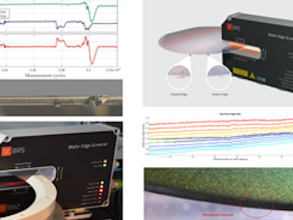
Wafer Edge Defect Inspection
Further information
Wafer Edge Defect Inspection
Production Level In-Line Measurement
Stand-alone wafer edge inspection
Integrated with cassette wafer loading
Profiling the wafer edge
Detection of broken and chipped wafer edges
Detection of micro cracks on the wafer edge
Detection of upper wafer edge defects or lower wafer edge defects
Application for opaque and transparent wafers
Classification according to SEMI Standards
Graphical output of visual inspection results
Log of wafer edge defects
MES data export
WordPress Cookie Plugin von Real Cookie Banner