Zum Inhalt wechseln
SEELANDSTRASSE 3, HS.4
23569 LÜBECK
INFO@KITEC.DE
+49 451 70323007
Home
Metrology
Non Contact Resistance and Resistivity Measurement
Metrology and Wafer Inspection
Wafer Edge Defect Inspection
Visual Wafer Inspection
Wafer Handling Systems
Wafer Transfer Systems
Wafer Tools
Wafer Sorter
Wafer ID Reader
Vacuum Wands
Process Tool Automation
Contact
Home
Metrology
Non Contact Resistance and Resistivity Measurement
Metrology and Wafer Inspection
Wafer Edge Defect Inspection
Visual Wafer Inspection
Wafer Handling Systems
Wafer Transfer Systems
Wafer Tools
Wafer Sorter
Wafer ID Reader
Vacuum Wands
Process Tool Automation
Contact
Metrology and Wafer Inspection
Further information
Different Application such as:
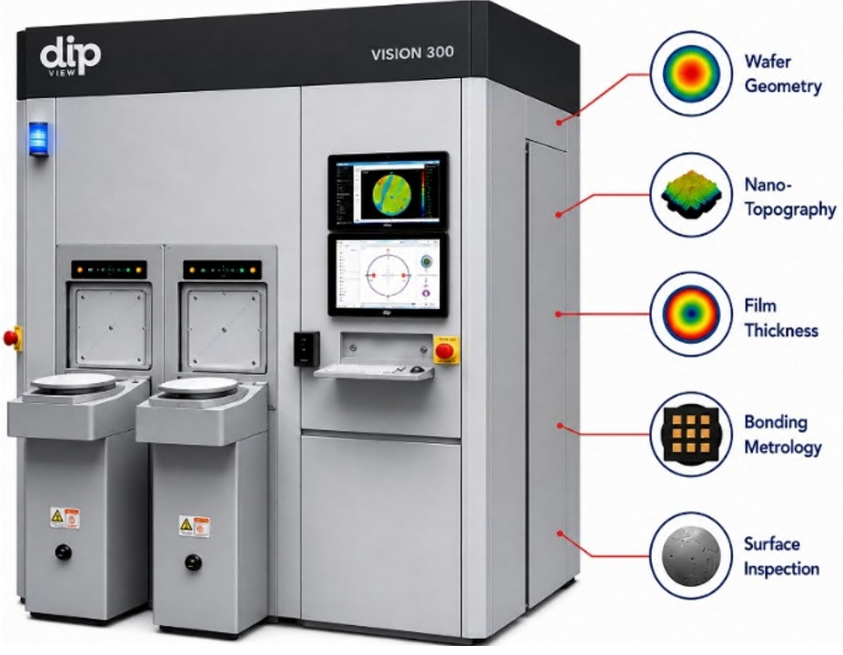
Integrated Wafer Metrology Platform and Wafer Inspection
Five Integrated Measurement Domains
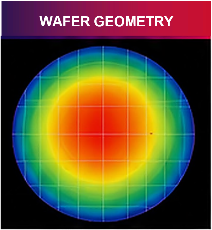
WAFER GEOMETRY
Bow/warp/TTV
SFQR
Edge-Roll-Off
Global shape
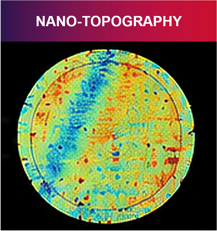
NANO-TOPOGRAPHY
Local flatness
CMP monitoring
Surface texture
Roughness
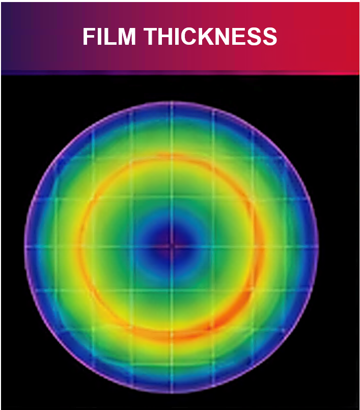
FILM THICKNESS
Thin transparent films
Thickness mapping
Uniformity
Stress induced
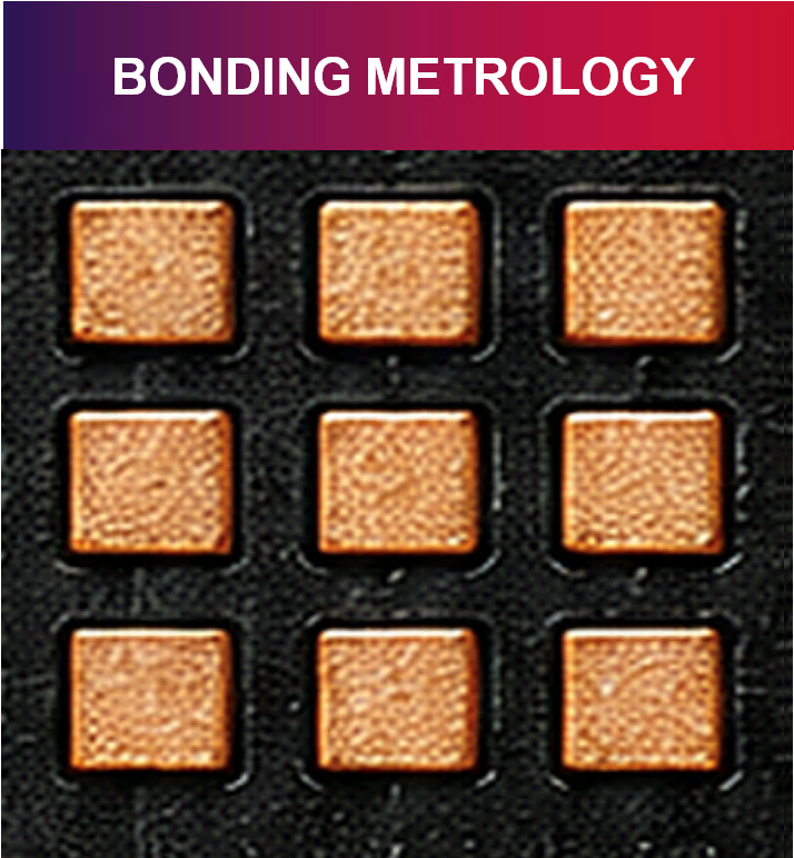
BONDING METROLOGY
Pre-bonding shape
Void Risk assessment
Chip tilt / warpage
Edge delaminations
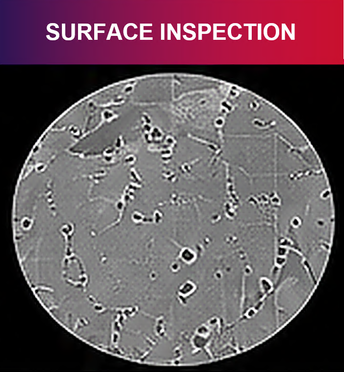
SURFACE INSPECTION
Surface Macro-defect
Particles
Scratches
Pattern Breaks
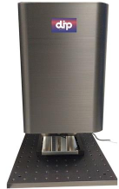
DIP-View VISION
Small Samples
manual loading
DIP-View VISION
up to 300mm wafer sizes
manual loading
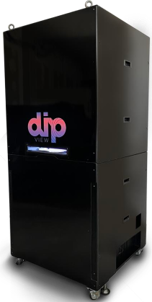
DIP-View VISION 200/300
up to 300mm wafer sizes
automatic operating
WordPress Cookie Plugin von Real Cookie Banner