Zum Inhalt wechseln
SEELANDSTRASSE 3, HS.4
23569 LÜBECK
INFO@KITEC.DE
+49 451 70323007
Home
Metrology
Non Contact Resistance and Resistivity Measurement
Optical Defect Inspektion
Wafer Edge Defect Inspection
Visual Wafer Inspection
Wafer Transfer Systems
Wafer Handling Systems
Wafer Tools
Wafer Sorter
Wafer ID Reader
Vacuum Wands
Process Tool Automation
Contact
Home
Metrology
Non Contact Resistance and Resistivity Measurement
Optical Defect Inspektion
Wafer Edge Defect Inspection
Visual Wafer Inspection
Wafer Transfer Systems
Wafer Handling Systems
Wafer Tools
Wafer Sorter
Wafer ID Reader
Vacuum Wands
Process Tool Automation
Contact
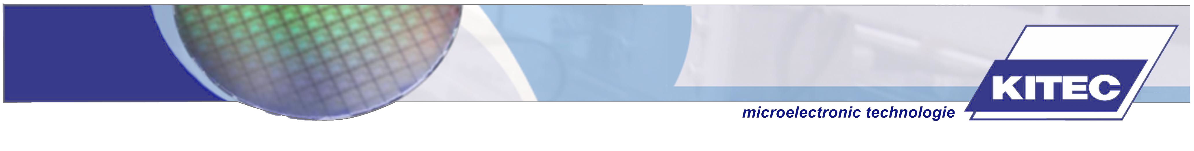
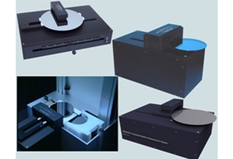
Non Contact Resistance and Resistivity Measurement
Further information
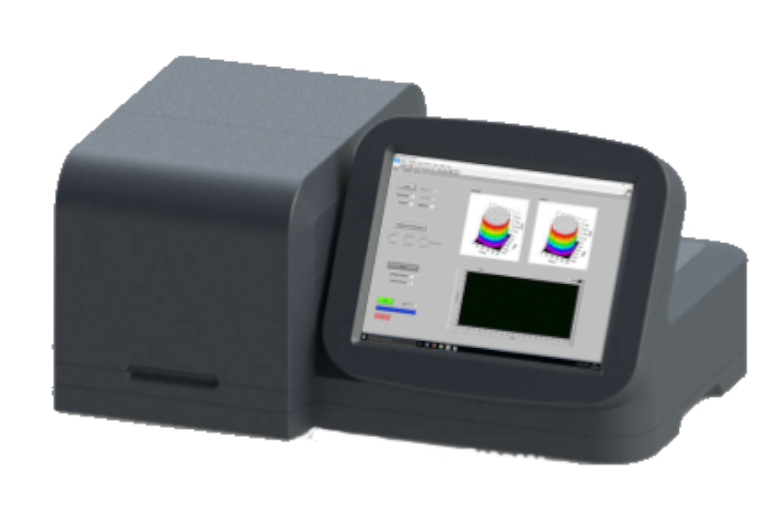
M-Res
Measurement system for semiconductor applications
Non-contact resistance and resistivity measurement system for low resistivity samples and high resistivity samples
Resistivity range from as low as 1mOhm up to 100kOhm
Resistivity mapping capability
Wafer diameter up to 300mm
Wafer thickness up to 2mm
PV-R / PV-RT – PVR-HF / PVR-HF P/N
Production Level In-Line Measurement
Non-contact resistance and resistivity measurement system
Resistance Range: 10Ohm – 200Ohm
Application such as production monitoring or quality control of PV wafer
Linien-Scan resistance variation monitoring
Option with integrated wafer thickness variation monitoring
Option of conductivity type monitoring
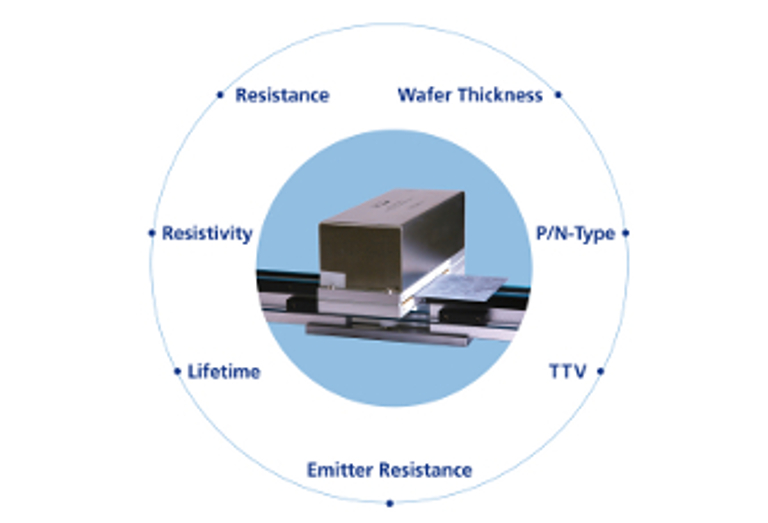
LCD-R
in-line measurement system for production lines
non-contact and non-destructive resistance measurement
measurement range: 0,1Ohm – 2000Ohm
application for manufacturing or quality control of coating process
MuTauScan
Resistivity and charge transport properties mapping system
For wafer size up to 150mm
Minimum wafer thickness 0,5mm
Non-contact and non-destructive method
Resistivity from 105 – 1011 Ωcm
Multi-function-detection head - measuring both resistivity and charge transport without changing wafer position
WordPress Cookie Plugin von Real Cookie Banner