Zum Inhalt wechseln
SEELANDSTRASSE 3, HS.4
23569 LÜBECK
INFO@KITEC.DE
+49 451 70323007
Home
Metrology
Non Contact Resistance and Resistivity Measurement
Optical Defect Inspektion
Wafer Edge Defect Inspection
Visual Wafer Inspection
Wafer Transfer Systems
Wafer Handling Systems
Wafer Tools
Wafer Sorter
Wafer ID Reader
Vacuum Wands
Process Tool Automation
Contact
Home
Metrology
Non Contact Resistance and Resistivity Measurement
Optical Defect Inspektion
Wafer Edge Defect Inspection
Visual Wafer Inspection
Wafer Transfer Systems
Wafer Handling Systems
Wafer Tools
Wafer Sorter
Wafer ID Reader
Vacuum Wands
Process Tool Automation
Contact
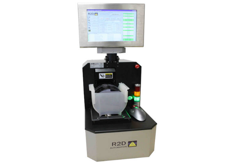
Wafer ID Reader
Further information
Wafer ID Reader
Reading wafer ID at the frontside, backside or both sides
12” Touchscreen
Visual representation of wafer ID with corresponding to its slots
For Cassette with 25 Slots
Cogned 1741 or 1742 OCR
Automatic mapping system
TCP/IP host connection
Possible Options: SECS/GEM Kommunikation / Automatic BCR or RFID
WordPress Cookie Plugin von Real Cookie Banner