Zum Inhalt wechseln
SEELANDSTRASSE 3, HS.4
23569 LÜBECK
INFO@KITEC.DE
+49 451 70323007
Home
Metrology
Non Contact Resistance and Resistivity Measurement
Optical Defect Inspektion
Wafer Edge Defect Inspection
Visual Wafer Inspection
Wafer Transfer Systems
Wafer Handling Systems
Wafer Tools
Wafer Sorter
Wafer ID Reader
Vacuum Wands
Process Tool Automation
Contact
Home
Metrology
Non Contact Resistance and Resistivity Measurement
Optical Defect Inspektion
Wafer Edge Defect Inspection
Visual Wafer Inspection
Wafer Transfer Systems
Wafer Handling Systems
Wafer Tools
Wafer Sorter
Wafer ID Reader
Vacuum Wands
Process Tool Automation
Contact
Optical Defect Inspektion
Further information
Optical Defect Inspektion
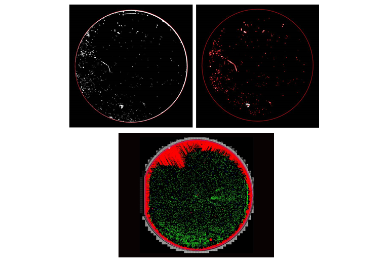
Optical inspection for marco defects and micro defects
Visual information of defects and their mapping
Systems with manual wafer handling and automatic mapping function
Bare and pattern samples
Wafer on dicing tapes
Dies in Waffle packs
nSpec LS defect inspection
Semi-automatic defect inspection system
Defect inspection for: Substrate wafer / EPI wafer / patterned wafer / Diced wafer / Dies and Individual samples
Create different receipt with rapid scanning, mosaicking user-specific way for presenting results, defect classification
Save image data for records or additional image processing with different parameter settings
Result data communication with different communication formats, e.g. KLARF
High resolution microscope with object lenses from 2,5x to 50x
LED lightning for BF;DF and DIC, transmitted light option
Motorized X/Y-Stage with 0.04µm increment
Wafer chuck for 2”,3”, 100mm, 150mm and 20mm or other sample holder available
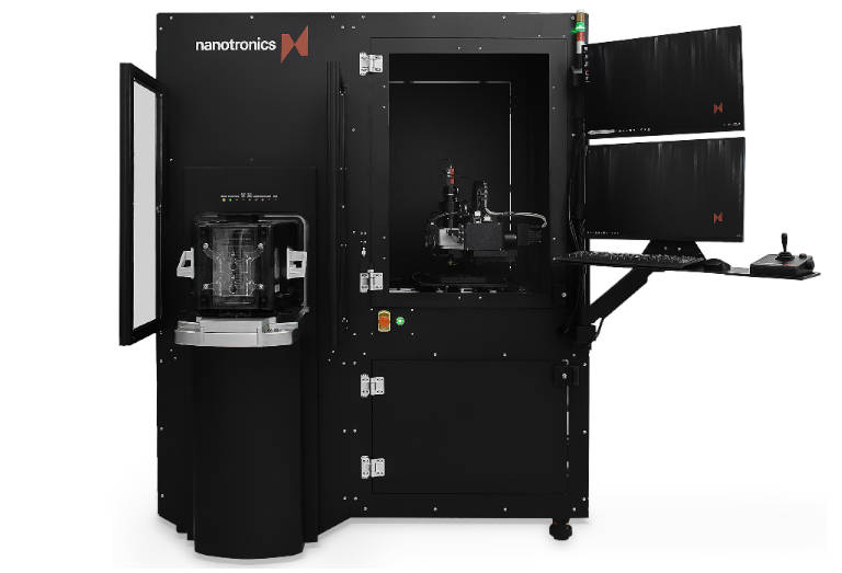
nSpec PS defect inspection
Automatic defect inspection
Defect inspection for: Substrate wafer / EPI wafer / patterned wafer / Diced wafer / Dies Individual samples
Create different receipt with rapid scanning, mosaicking user-specific way for presenting results, defect classification
Save data as e.g. KLARF or CSV
High resolution microscope with objective from 2,5x to 50x
LED lightning for BF;DF and DIC, transmitted light option
Motorized X/Y-Stage with 0.04µm increment
Wafer chuck for 2”,3”, 100mm, 150mm and 20mm or other sample holder
Wafer loader with pre-aligner
Carrier and wafer size detection
OCR reader option
GEM/SECS Option
nSpec CPS
Automatic defect inspection
Defect inspection for: Substrate wafer / EPI wafer / patterned wafer / Diced wafer / Dies Individual samples
Create different receipt with rapid scanning, mosaicking user-specific way for presenting results, defect classification
Save data as e.g. KLARF or CSV
High resolution microscope with objective from 2,5x to 50x
LED lightning for BF;DF and DIC, transmitted light option
Motorized X/Y-Stage with 0.04µm increment
Wafer chuck for 100mm, 150mm , 200mm, 300mm
Wafer loader with pre-aligner
Carrier and wafer size detection
OCR reader option
GEM/SECS option
WordPress Cookie Plugin von Real Cookie Banner